 |
Voltage Stabilizer Patent BY1860C1 |
 |
|
 |
| Wal Design group |
|
The voltage stabilizer
(informal translation)
The invention concerns to the area of voltage stabilizers and can be
used at the power supplies and measuring devices development.
The linear voltage stabilizer is known. This is a system of automatic
control. This stabilizer supports the constant voltage on output with given
accuracy. And this voltage does not depend on the parameters of circuit.
(1). But this stabilizer has low accuracy of stabilization, because any
change of a reference voltage repeats by the output voltage.
Closest to offered (prototype) is the stabilitrone of forbidden zone,
on base "current mirror". It contains divider, stabilitrone with
a voltage "of forbidden zone" and comparing circuit with regulating
element. In this device for increasing of stabilization accuracy, the voltage
of base transition of the transistor sums up with a voltage created by
a pair of transistors, working with some ratio of currents density (2).
Lack of the known device is low accuracy of stabilization, because
the parameters of the pair transistors have to be absolutely identical.
It limits the accuracy of stabilization.
The problem of invention - to increase the accuracy of voltage stabilization,
irrespective of the circuit parameters.
This problem is reached by that into the voltage stabilizer (which
contains a divider, comparing circuit with regulating element, the output
of which is connected to the input of divider, and the first input of comparing
circuit with regulating element is for the input voltage) are in addition
entered the voltage inverter and voltage to current converter. The input
of voltage to current converter is connected to the output of divider,
and the output is connected to the input of voltage inverter, the output
of which is connected to the second input of comparing circuit with regulating
element, and the third input of comparing circuit with regulating element
is connected to zero potential (ground).
The voltage inverter has two resistors and a diode optocoupler. The
first end of second resistor is the output of voltage to current converter,
and the second end of second resistor is connected to the first end of
first resistor and to the anode of radiating diode. The cathode of which
is connected to zero potential (ground) and to the anode of photo diode,
the cathode of which is connected to the second end of first resistor and
is the output of voltage inverter.
The technical result of invention is to decrease the instability of
output voltage, due the external revolting factors (for example the temperature),
up to indefinitely small size. It is possible, because the system of regulation
does not contain any reference, it finds the zero of variable signal, that
is possible to make rather precisely.
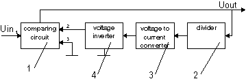
The invention is explained by the diagrams, where:
The pic.1 has the block diagram of voltage stabilizer.
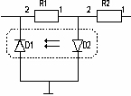
The pic.2 has a variant of the voltage inverter.
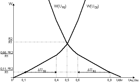
The pic.3 has the transfer function of voltage inverter.
The device contains the comparing circuit with regulating element 1/pic.1/,
divider 2, voltage to current converter 3 and the voltage inverter 4. The
first input of comparing circuit with regulating element 1 is for voltage
Uin, and the output of comparing circuit with regulating element has the
output voltage Uout. Uout also is going to the input of divider 2, from
the output of which the signal is going to the input of voltage to current
converter 3. The output of voltage to current converter is connected to
the input of voltage inverter 4, the output voltage of which is going to
the second input of comparing circuit with regulating element 1, where
it compares with zero potential at the input 3, amplifies and in the necessary
phase influences the regulating element.
The voltage inverter 4 contains the diode optocoupler D1, D2 /pic.2/
and two resistors R1, R2. The first end of R2 is the output of voltage
to current converter 3/pic .1/, and the second end of R2 /pic.2/ is connected
to the first end of R1 and to the anode of radiating diode D2. The cathode
of which is connected to zero potential (ground) and to the anode of photo
diode D1, the cathode of which is connected to the second end of R1 and
is the output of voltage inverter 4/pic.1/.
The device works as follows. The input voltage Uin is going to the
first input of comparing circuit with regulating element 1/pic.1/ where
the part of voltage falls, and from an output of comparing circuit with
regulating element the output voltage Uout is going to the divider 2. Uout
is the output voltage of stabilizer.
Divider 2 divides Uout in any given ratio. From the output of divider
the signal is going to the input of voltage to current converter 3. The
voltage to current converter 3 transforms the voltage of divider Udiv to
the current I2. The current I2 is going to the input of the voltage inverter
4, where passes by the circuit R2, D2 /pic.2/.
Current I2 can be described by equation:
| Udiv |
UR2+UD2 |
Udiv-UD2 |
| I2= |
---------------- = |
--------------------- = |
------------------- ; |
|
r2+R2 |
r2+R2 |
R2 |
Where:
UR2 - voltage across R2;
UD2 - voltage across D2;
r2 - internal resistance of D2.
The passage of a current through the circuit R2, D2 generates a voltage
in the photo diode D1 and in the circuit R1, D1. The current I1 is the
current across R1, D1. The current I1 creates a voltage failure dUD1 on
the diode D1 1/pic.1/, which is going to the second input of comparing
circuit with regulating element, where it compares with zero potential
at the input 3, amplifies and in a necessary phase influences the regulating
element as long as potentials at the inputs two and three (of the comparing
circuit with regulating element 1) will not become equal, that will bring
system in balance and Uout will be determined, as the function from Udiv.
Udiv, from the formula for I2 is defined by dependence: Udiv=UD2 + UR2;
In this condition the voltage inverter transfer function /pic.2/ looks
like:
|
UD2*R2
|
(Udiv-UR2)*R2
|
|
W=
|
------------------------ =
|
------------------------- ;
|
|
(Udiv-UD2)*R1
|
UR2*R1
|
From the diagram of this function /pic.3/ it is visible, that if for
D2 working area of /pic.2/ will correspond, for example, left bottom part
of the diagram /pic.3/, then the change of UD2 on size dUD2 will be absolute
linearly and opposite by the phase to change UR2 on size dUR2. When the
entrance voltage Uin /pic.1/, output voltage Uout, and the circuit parameters
changes, Udiv will change on size dUdiv, or UD2 will change on size dUD2,
that will effect, that UR2 will change on size dUR2.
This dependence describes by equation:
Udiv±dUdiv=(UD2±dUD2)+(UR2±-dUR2) ;
But if ±UD2±-UR2=0 /pic.3/, then ±dUdiv=0.
Accordingly the output voltage Udiv of divider 2/pic.1/ always keeps
the primary value, which depends only on chosen variant of voltage inverter
4 and ratio of two resistors R1, R2 /pic.2/. So, Uout is a constant.
Thus, in this system of regulation the output signal of voltage inverter
4/pic.1/, by working the voltage to current converter and the comparing
circuit with regulating element 1, compensates up to zero potential. And
the accuracy of stabilization raises.
Diagrams
pic.1
pic.2
pic.3
The formula of invention
1. The voltage stabilizer contains a divider, comparing circuit with
regulating element, the output of which is connected to the input of divider.
The first input of comparing circuit with regulating element is for the
input voltage. The stabilizer in addition has a voltage inverter and a
voltage to current converter, and input of the voltage to current converter
is connected to the output of divider, and the output of the voltage to
current converter is connected to the input of voltage inverter, the output
of which is connected to the second input of comparing circuit with regulating
element, and the third input of of comparing circuit with regulating element
is connected to zero potential (ground).
2. The voltage stabilizer by p.1, has the voltage inverter, which contains
two resistors and a diode optocoupler. The first end of second resistor
is connected to the output of voltage to current converter, and the second
end of second resistor is connected to the first end of first resistor
and to the anode of radiating diode, the cathode of which is connected
to zero potential (ground) and to the anode of photo diode, the cathode
of which is connected to the second end of first resistor and is the output
of voltage inverter.
© Alexey Stratilatov 1998
[email protected]
ADVERTISING

| |
This site is private property not for copy, sale or rental until you have unless money. All matherials on this site are for personal use only.
© Alexey Stratilatov 1998, [email protected].
|